.jpg)

.jpg)

 English daily published in Bengaluru & Doha

IIIT students make breakthrough in indigenous chip design
Hubballi,
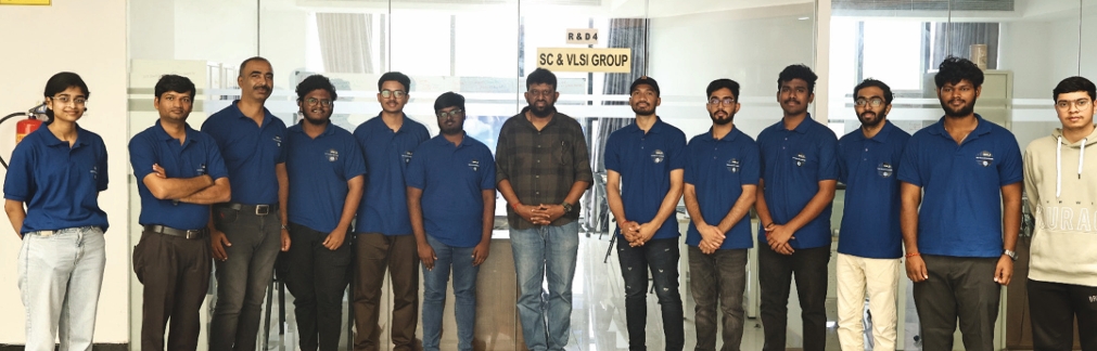
In a major push for indigenous technological innovation, a team of 12 final and pre-final year engineering students from the Indian Institute of Information Technology (IIIT) has successfully designed a custom 180nm silicon chip. Named ‘SIDHARUD1’, the chip has been selected as part of a prestigious global chip tape out program, making the institution one of the few select cohorts globally to achieve this milestone.
The project was executed under a highly competitive global joint collaboration organized by GlobalFoundries, a semiconductor manufacturing giant based in Germany, and Synopsys, a leading electronic design automation (EDA) software vendor. Out of 55 teams qualified worldwide, the IIIT student team secured a spot as one of only six teams selected from India.
The chip addresses a common hardware limitation in modern computing. Standard microprocessors and microcontrollers on a computer board run critical software but are restricted by a fixed number of physical pins (often limited to 40 pins), making it incredibly difficult to connect additional devices or sensors as system demands grow. The newly developed 'SIDHARUD1' chip acts as a GPIO (General Purpose Input Output) expander.
Utilizing the open source I2C communication protocol, the chip requires just two physical wires to connect alongside a host microproces sor, instantly expanding its capacity to manage an additional 25 peripheral devices (comprising 16 inputs and 9 outputs). Furthermore, the architecture is scalable; combining four of these chips can scale a system's capacity to handle up to 100 inputs seamlessly.
Beyond expanding connectivity, the chip features programmable capabilities and can perform localized data pre-processing, such as filtering out data noise, before information even reaches the main processor. The entire architecture was devel oped using a RISC-V open-source processor core, eliminating dependencies on expensive, proprietary paid Intellectual Property (IP). Speaking on the develop ment, Dr. Jagadish D.N., As sistant Professor and the lead project coordinator, said that the accomplishment highlights the design capabilities of the students.
"The complete design was driven by our students. Rather than relying on restrictive, paid commercial IPs, they utilized open-source frameworks— reminiscent of premier national initiatives like IIT Madras' 'Shakti' processor. They wrote custom code, ran exhaustive simulations, and successfully finalized the layout for production." The intensive project spanned from May to September, at which point the final design was frozen and submitted for "tape-out" (the final logic design phase before manufacturing).
The chip is currently undergoing physical fabrication at GlobalFoundries' facility in Germany and is expected to arrive at the campus fully packaged within a month for hardware testing. The student cohort was heavily backed by industry expertise throughout the development lifecycle. Alongside academic guidance from Dr. Jagadish, the team received technical mentorship from prominent industry leaders, including Dr. Anand Bariya of the Deshpande Foundation and Santosh Devanallikar from Nokia. Director IIIT-Dharwad, SR Mahadeva Prasanna hailed the efforts of the students and congratulated them for their achievement. The IIIT team attributed the success to the director for his mentorship, constant encourage ment and support by setting up the VLSI ecosystem and seeding the much needed minor degree specialization in VLSI.

.jpg)

.jpg)